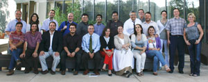
Nanotechnology Workshop: Reading Materials
3rd UTEN Workshop 2010 - Nanotechnology
Research Collaboration & Network Building for Commercialization in NanoSciences
University of Minho - 15-16 November, 2010
Program | Venue | Speakers | Reading Materials | Photos
The nanotechnology economy (www.nanoforum.org)
It is an undisputable fact that nanotechnology is gaining ever more interest, even from the financial community: in 2007 over $US 4 billion were spent in Nanotechnology research worldwide. Nanotechnology covers various industries and enables various technologies; however the highest activity has been seen in nanoelectronics, the energy sector and solutions for personal and health care products.
Nanoelectronics has been leading the patenting landscape due to the continued drive towards miniaturisation. The innovation process in nanoelectronics is lead by Japan followed by the US. The Semiconductor Industry Association has made a conservative estimate of the nanoelectronics market to reach $300 billion by 2008.
Nanotechnology applications have been touted as the most promising for novel solutions to our current energy problems. These include materials for hydrogen storage, polymer membranes for fuel cells, and semiconductors for solar cells. The application of nanotechnology in the health and personal care sectors has
seen the emergence of niches such as cosmeceuticals and nutraceuticals .
Several questions from various perspectives remain unanswered and challenges unresolved.
• Will nanotechnology patenting live up to its promise or become a litigation minefield?
• Will the ranks of academic researchers maintain their integrity in the face of ever increasing commercial pressures for patenting?
• Will patent offices across the world be able to stand up to the challenge of ensuring that invalid, too broad or overlapping patents are not issued?
• Will society be able to bridge the nano-divide, sharing the benefits of envisaged wealth creation?
Challenges of nanotech commercialization (www.nanoforum.org)
The transfer of Nanotech knowledge into commercially available products needs to match the present high expectations around the nanotechnology economy.
The main challenge of the technology transfer profession in this domain is coping with the specific character of nanotechnology as a research area. According to the NanoForum report below, the major barriers to the transfer of nanotechnology to industry are the following:
• On one hand, people and skills, ie, the difficulties of building an ideal nanotechnology transfer team with a combination of skills in physics, chemistry, biology, materials science, modelling, business and management. The communication barriers resulting from such broad range of fields leads to a poor understanding of what nanotechnology is.
• On the other hand, long term public and regional strategies based on excellence: To develop efficient technology transfer incubators or networks one may need over 10 years work by a community of scientists, administrators, local authorities and business, with strong leadership.
In Europe, and the regarding the nanotech innovation ecosystem, further barriers need to be addressed. According to a report of the Nanoforum workshop on the commercialisation challenges of Nanotechnology that took place in Helsinki, Finland on March 29th 2007, three areas of concern for Europe are identified: venture capital, patents granted and industrial investment:
• A very low proportion (only 3,5%) of global nanotechnology venture capital is invested in Europe.
• Despite public funding which is on a par with the US, Europe is lagging behind in the number of nanotechnology patents granted.
• Industrial investment in nanotechnology is also only half that of the US and Japan.
Nanotechnology Commercialisation (Nanoforum Workshop Report, Tom Crawley, 2007)
The low level of venture capital is largely due to a shortage of suitable investment targets. Companies lack focused business models, commercial experience, and exit strategies. Whilst public funding sources may take the place of venture capital, the concern is that companies then lose the other benefits that investors would bring, such as in-depth industry understanding and networks. Low patent productivity is a consequence of the difficulty of identifying the commercial potential of research, partly because research is not aligned to industrial needs. There are specific questions of motivation (publications being more highly prized) and patenting capability. The explanation for low industrial investment, despite the presence of nanotechnology ‘global leaders’ among European industry, is a failure to activate wider industrial interest. A company contemplating an investment in nanotechnology development will be dissuaded by the obvious challenges (production scale-up, health and safety concerns) if they do not understand the less obvious opportunities that nanotechnology brings.
The three challenges have a common solution.
The investment of public funding in nanotechnology development needs to enable a greater amount of funding from private sources. In order for this to happen, there needs to be an understanding of the industrial or consumer problems which need to be solved, which then need to be fed back to development and research. This can be done in several ways:
• Technology-led ‘roadmapping’ should be augmented by industry-led ‘visions’ which set out real industrial challenges.
• Funding priority should be given to projects which meet those challenges, and which combine academic and industrial participants.
• Researchers should be incentivised to product patents as well as publications, by sharing in the profits of licensing or other exploitation.
• Universities should be able to rapidly assess the value of a potential patent, which is enabled by understanding the needs that must be solved.
• Individual firms should take their nanotechnology-based processes and rather than attempt to apply it in multiple applications and industries, focus on the area of greatest need. They should then understand with what or whom they need to integrate, in order to provide a whole solution.
• Investors should apply their industrial knowledge and networks to help nanotechnology companies develop, a contribution which may be as valuable as a financial investment.
• Finally, the wide range of European industry that has not yet been ‘activated’ should also take responsibility for understanding the opportunities of nanotechnology, and identifying with whom they need to partner in order to meet those opportunities.
Nanotechnology Commercialisation (Nanoforum report, 2007)
Abstract: This is a report of the Nanoforum workshop on the commercialisation challenges of nanotechnology. The workshop took place in Helsinki, Finland on March 29th 2007. According to a report of the Nanoforum workshop on the commercialisation challenges of Nanotechnology that took place in Helsinki, Finland on March 29th 2007, three areas of concern for Europe are identified: venture capital, patents granted and industrial investment:
• A very low proportion (only 3,5%) of global nanotechnology venture capital is invested in Europe.
• Despite public funding which is on a par with the US, Europe is lagging behind in the number of nanotechnology patents granted.
• Industrial investment in nanotechnology is also only half that of the US and Japan.
Recommendations for Business Incubators, Networks and Technology Transfer from Nanoscience to Business (Nanoforum report, 2007)
Abstract: The industrial and commercial application of scientific research is a subject of intense debate in Europe. The motivation is clear: industrial competitiveness depends to a large extent on access to high technology. Scientific research in publicly funded laboratories is a potential source of new technologies. The problem of efficient technology transfer is a particularly important issue for nano science and technology because of its very rapid development in the past decade.
Summary: This report is the result of the two day workshop “Nano2Business” held at Warsaw University of Technology on 7th and 8th February 2007. The main focus of the discussions was on the best organisation for technology transfer incubators, technology transfer networks, and on identifying the main barriers to technology transfer. The issue of specific aspects of nanotechnology transfer was discussed. The report gives recommendations for creating good technology transfer incubators, and examples of incubators, networks and technology commercialisation strategies. The nanotech-aspect of technology transfer is discussed. Attention is given also to barriers for nanotech and technology transfer in general with regards to the way research is organised and research organisations evaluated.
Intellectual Property in the Nanotechnology Economy: trends, patent landscape and the challenges (Nanoforum report, 2007)
Abstract: Article outlines the roles of Intellectual Property in the developing Nanotechnology Economy. It covers an introduction to the subject, the emerging trends, patent landscape and the outstanding challenges to be resolved.
Summary: The increasing move towards a knowledge-oriented economy, the role of intellectual property is poised to increase wealth creation, growth and development through the application of new technology across the world.
Trends in Nanotechnology IP
• Patents are being filed on fundamental building blocks, materials and tools from the outset of technology development. The US patent office has received applications with claims regarding the composition of matter, devices, apparatus, systems and control of nanomaterial and devices, and methods.
• Cross-industry patent claims are being made for single nanoscale innovations that may have diverse applications. Applications have been identified in major patent classes such as electricity, human necessities, chemistry and metallurgy, performing operations and transporting, mechanical engineering, physics, fixed construction, textiles and paper.
• Universities and public research foundations hold a large proportion of nanotechnology patents that will be essential for nanotechnology products, according to Stanford Law School Professor Mark Lemley. It is estimated that universities hold 70% of key nanotechnology patents. Before 1980, 250 nanotechnology-related patents were granted annually to universities worldwide. By 2003 this number had increased 16-fold to 3993.
• Patenting on natural products used as herbal medicines is increasing. For example, a Chinese researcher Yang Mengjun has reduced traditional Chinese medicinal herbs to nanoscale formulations and claimed exclusive monopoly to 900 patents. Such patents have been granted in US and Europe with one such example being the Korean Pacific Corporation’s European patent on nanoscale ginseng for use in cosmetic products.
• A marked increase in US patents being filed from Indian research laboratories, demonstrating a dramatic change in the research culture on the subcontinent. The annual number of US patents produced by the 38 Indian national laboratories has increased from 30 in 1995 to 720 in July 2006.This trend has also been observed in large multinationals such as IBM, Intel, General Electic, General Motors, Cisco and Sun Microsystems, which are setting up research centres in India. Public and private laboratory patents are rapidly transforming in turn into licences.
Nanotechnology in Europe - Ensuring the EU Competes Effectively on the World Stage (Nanoforum report, 2007)
Abstract: This is a report of the Nanoforum survey and workshop organised to identify barriers to the commercialisation of nanotechnology in Europe. The report offers advice as to what measures could be put in place to remove such barriers so that the benefits of new products and processes beneficial to society can be realised. The workshop was the final of three commercialisation workshops and took place during EuroNanoforum in Düsseldorf on 21st June 2007.
Summary: Many recommendations are made in this report to encourage the commercialisation of nanotechnology in Europe and it is evident that this is desired as there is a huge potential for application driven technology commercialisation. Key recommendations are summarised in the report, however there is a desire for: • More application driven funding for nanotechnology • Less fragmented networks and consolidation of efforts • More training and communication activities • Guidance on successfully implementing self-sustaining framework projects There is also a desire to capitalise on FP6 and FP7 funding and what is suggested is that Europe develops it own strategy with less emphasis on national strategies.
Nanotechnology Skills and Training Survey. Summary of Outcomes (Nanoforum report, 2007)
Abstract: The objective of the nanotechnology skills and training survey was to identify the skills gaps and training needs of the workforce in the emerging area of nanoscience and nanotechnology. It also aimed to identify the current and prospective roles of graduates and post-graduates, along with the professional development needs. An intended outcome of the survey is to inform education and training Institutions of the gaps and latent needs. The scope of survey included organisations from industry, government bodies, non-governmental sector and training institutions.
Summary: This report contains a summary of outcomes from the quantitative analysis of results. A total number of 240 responses were received, that were classified into three categories of clear and coherent, incomplete, and incoherent and invalid responses. The qualitative analysis was based on 186 responses after excluding the invalid responses. A majority of respondents are involved in management or research based roles at government institution, not for profit bodies, large and micro sized companies. 79% of these respondents use nanoscience and nanotechnology knowledge in their organisational programs, services and products. A range of roles have been identified for nanotechnology graduates and post-graduates. Doctoral qualifications were considered to be the knowledge level of preference. The responses indicated that both generalist and specialist skill sets were valued by employers. The survey indicated that knowledge of nano-science for engineers was relatively more important than knowledge of engineering concepts for science graduates and post-graduates. The survey indicated that the three relatively important natural science competencies were knowledge of material science, nano-biology interface and nanoscle effects. A relative comparison of fabrication, charecterisation and other technical competencies has been presented. A relative comparison of commercial, management and societal knowledge competencies has also been presented. Knowledge of research and development management, and project management were considered very desirable. A comparison of languages and soft skills has been presented in the report. Team working and good verbal communication were considered very desirable soft skills.
Promotion of Long-Term Relationships with Companies: The Technological Platform IDPoR (Research and Development in Polymers from Renewable Sources)
IDPoR, an association between academy (CICECO lab) and industry, was created in September 2006, but it was in 2007 that it revealed itself as an outstanding example of technology transfer and applied research.
The main purpose defined for IDPoR was to carry out investigations related to the synthesis, characterisation and possible applications of novel polymeric materials derived from the chemical exploitation of vegetable and animal biomass. With the increasing regular intervention of our associated companies, namely Caima, CIN, SA, Euroresinas – Indústrias Químicas SA (Sonae Indústria), RAIZ (Portucel Soporcel group), Resiquímica – Resinas Químicas SA and SAPEC Química SA, two main strategies have been covered, viz. a more fundamental approach through doctoral Theses, aimed at opening new avenues and assessing their potential, and a more applied approach intended to tackle concrete issues of our associates’ direct interest. Whereas the first aspect bears the connotations of a typical academic context and is therefore conducted as an ‘open research’, the second has been developed in the form of confidential projects sponsored by the industrial partners. Although these have priority in the implementation of specific confidential research projects, IDPoR was contacted by companies, other than associates, in order to perform simple sample analysis, or develop deeper studies. These contracts gave IDPoR, in the first place, the opportunity to gain experience in this field and helped, secondly, the platform to pursue financial sustainability.
Another fundamental role of IDPoR, was the organization of training courses for post-graduate students and industrial cadres. Finally, an important disseminations means of IDPoR has been its website (http://idpor.ciceco.ua.pt), which covers bibliography, technical news items and other relevant topics, as well as a reference to specialised courses and seminars proposed by IDPoR.
Flexible Germanium Nanowires: Ideal Strength, Room Temperature Plasticity, and Bendable Semiconductor Fabric
Damon A. Smith, Vincent C. Holmberg, and Brian A. Korgel (ACS Nano, 2010)
Abstract: We have developed a solvent-based approach to VLS-like growth of semiconductor nanowires, called supercritical fluid-liquid-solid (SFLS) growth, which enables the production of large amounts of nanowires. For example, more than 1g of Ge nanowires can be produced in a single reaction in a 250mL vessel. This approach provides enough material to explore new applications of semiconductor nanowires, like fibers and fabrics.
Nanowires of materials that are typically brittle, are flexible and strong, and can exhibit a distinctive combination of electronic, optical, andmechanical properties, important for a variety of new device technologies, including next generation flexible electronics, nano electromechanical systems (NEMS), piezoelectronics, and structural materials.
The large quantity of Ge nanowires produced by the SFLS method and their high flexibility allows for the fabrication of nonwoven ceramic fabric, or paper, of Ge nanowires.
Ceramic Fabrics
(http://www.inventables.com/technologies/ceramic-fabric)
Currently, two kinds of ceramic fabrics are available, woven and non-woven (Nonwoven materials are shaped into mats of randomly oriented fibers). The non-woven material can be made as thin as paper. When exposed to open flame the organic binder used to manufacture it will discolor, but the material itself will be unaffected. The woven varieties are made of strong alumina-boria-silica fibers. In addition to outperforming other high temperature textiles when exposed to flame, woven ceramic fabrics also exhibit good mechanical properties.
The thin non-woven fabric has been used in the walls of airplanes as a flame barrier. Woven ceramic fabrics have been used for their fire protection properties in furnace curtains, but recently they were applied to the International Space Station to protect from micrometeorite collisions.
 UTEN RSS Feed
 UT Austin|Portugal on Twitter